Tell me a little about yourself!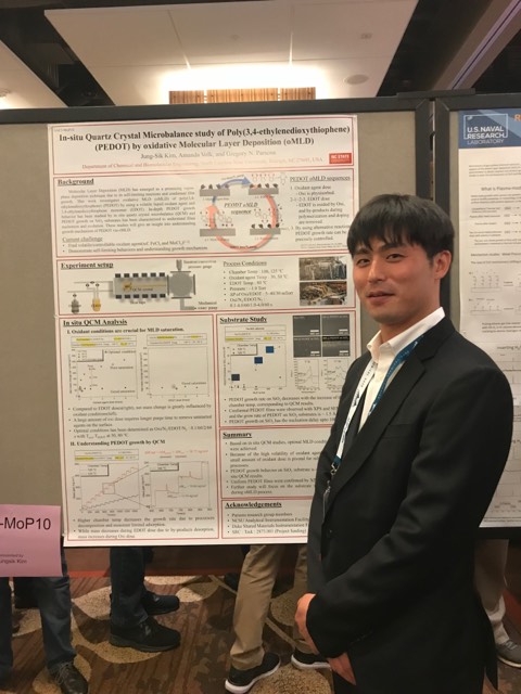
I am a third year PhD student in Chemical Engineering advised by Dr. Gregory Parsons. After graduation, I would like to work in an industry related with semiconductor field. Outside of the lab, I like to play soccer and watch all kinds of sports such as soccer, baseball, football, and basketball. Also, I like traveling; I have visited around 30 countries and my next destination is Africa.
What primary instrument(s) are you using for your research and what do you like about it?
I usually use the FEI Verios SEM and the FEI Talos F200X to characterize the surface morphology and film thickness. For TEM sample prep, I use the FEI Quanta 3D FEG. I also use the Rigaku Smartlab X-ray diffractometer for XRR to analyze film density and thickness, and X-ray photoelectron spectroscopy (SPECS system with PHOIBOS 150 analyzer) to evaluate the chemical composition of the film. These all measurement techniques are greatly helpful to understand and proceed my research.
What have you been researching and how is it impacting the community?
My research is to study the thin film growth behavior using atomic layer deposition (ALD) and molecular layer deposition (MLD). The thickness regime that I am interested in is under 100 nm scale, so SEM and TEM is particularly beneficial for my research. Since ALD/MLD is based on surface chemistry, the chemical selectivity depending on the different substrates enables to provide selective deposition on substrates. This is called as area selective deposition (ASD) and we are aiming to develop different ASD processes using different precursors and reactant agents.
“As the feature size of state-of-the-art transistor is becoming smaller, the conventional lithography technique faces a lot of technical challenges. As a pathway, ASD has drawn attention because it can provide self-aligned patterning without precise alignment steps. For these reasons, many semiconductor companies are trying to develop novel ASD processes using ALD/MLD processes.”

What have you learned from your experience at AIF?
FIB and SEM short courses allows me to understand the fundamental principle of FIB and SEM. Through these courses, I am able to understand what kind of operating condition is suitable for my interest. I strongly recommend to take the short course offered by AIF if you want to understand the technique more deeply.
Best thing about AIF in 5 words or less?
Awesome people and technical tools.
Is there a staff member at AIF that has helped you?
I thank all of the staff who trained me including Chris Winkler, Roberto Garcia, BB Chung, Chuck Mooney, Fred Stevie, Toby Tung, and Elaine Zhou. Specially, I owe a big thank to Chris, Roberto, and Fred for TEM and FIB.